Aflexible printed circuit is as much a mechanical device as it is an electrical device. Conductors must be laid out such that the circuit functions properly and reliably. Unlike a rigid printed-circuit board (PCB), flexible circuits bend, flex, and otherwise contort to fit the final assembly. These bending and flexing operations can severely strain improperly routed internal conductors.
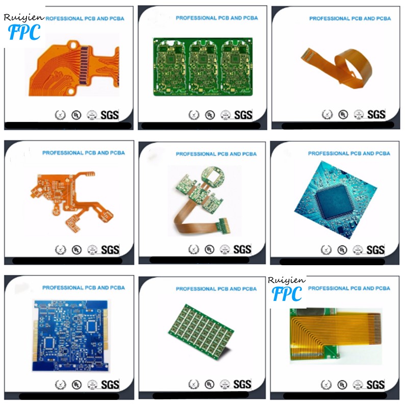
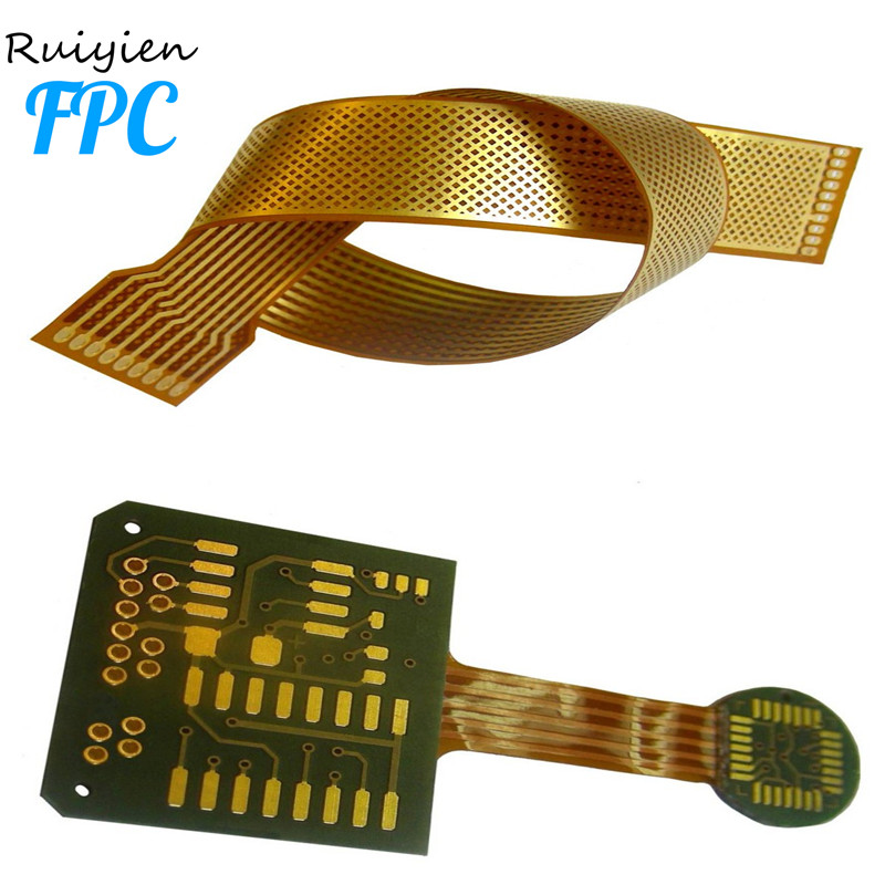
The industry standard IPC-T-50 of the IPC Association Connecting Electronics Industries defines a flexible circuit as, “A patterned arrangement of printed wiring utilizing flexible base material with or without flexible cover layers.” A typical flexible circuit is formed by stacking four different types of primary layers: the base layer, a metal foil or conductor layer, an adhesive layer that bonds the other layers together, and outer insulating (cover) layers. Multilayer boards stack these four basic layers as needed to complete the circuit design.
The base and cover layers are typically a flexible polymer
film that creates the foundation of the flexible circuit and provides most of the physical and electrical properties of the circuit. A number of materials may be used as base films, but most flexible circuits today use polyimide films because of their excellent electrical, mechanical, chemical, and thermal properties.
Normal base-material thickness typically falls between 12 and 125 μm (0.5 to 5 mils), but thinner and thicker bases are possible. It should be obvious that as the base material gets thinner, the circuit becomes more flexible.
The metal foil layer provides electrical connectivity for the circuit. While different metals may be used, the most common metal found in flexible circuits is copper. Its high malleability, along with good conductivity, makes it an ideal material for flexible applications.
Rolled and annealed (RA) foils are the most common choice, though thinner foils may use electrodeposited (ED) copper.
The bonding-adhesive film, as its name implies, affixes the metal foil layer to the base material, bonds base layers to each other, and also adheres covers to the circuit. As with base films, adhesive films are available in different thicknesses, which are usually determined by the application. For example, different adhesive thicknesses are used in the creation of cover layers to meet the fill-needs demanded by different thickness copper foils. The most-common adhesive films used today are made from a modified acrylic or epoxy base.
When circuits bend or flex, material towards the outside of the bend must stretch to cover the expanded radius, placing that material in tension. Materials inside the bend, however, see the force of compression as the inside-bend circumference shrinks.
At some point in the middle of the material stack is an area that sees little to no tension or compression. This area is called the neutral-bend axis. In a flex circuit, it’s loosely defined as an imaginary planar region with no thickness that undergoes neither tension nor compression during bending or flexing. As different layers in the flexible circuit move further away from the neutral-bend axis, the forces of tension and compression become more severe and damaging.
The neutral-bend axis may not be in the exact middle of the material stack. Material composition, thickness, and the amount of area covered by the material (as, say, a copper ground plane in one layer versus normal copper traces in another) can shift the neutral bend axis from the middle of the stack。
The
designer must generate a drawing package for many circuit designs. While it is important to completely specify critical features, don’t overspecify noncritical features of a drawing. Overspec’ing adds cost but does little to boost robustness.
Good drawings have a flat view of the circuit with critical dimensions only. Remember: Electronic data (Gerber, DXF, OBD++) will define every circuit feature. Before a manufacturer can begin the setup, the designer should always compare every dimension on the drawing to the electronic data before beginning setup. The FCB manufacturer and the customer must work out any discrepancies, which routinely happens prior to beginning circuit fabrication. Otherwise, discrepancies found after fabrication begins can easily add weeks to the lead time and often incur additional charges.
Don’t specify adhesive thickness on the drawing. The drawing should only specify overall thickness of the circuit and the overall thickness of critical dielectrics that impact impedance.
Every test specification on the drawing has an associated cost that adds to the final circuit cost. Many tests that verify critical electrical features of the circuit, such as continuity and insulation resistance, are standard. When selecting optional tests, however, make sure each test is worth its cost.
Whether a flexible circuit functions reliably when bent depends on many design factors, including the bend radii, dielectric type and thickness, foil weight, copper plating, number of layers, circuit thickness, and whether the application is static (bent once for a permanent installation) or dynamic (follows a hinged joint or other moving part).
Tight bend radii boost the probability of failure when the board is flexed. One method used to indicate bend-radius reliability is the bend-radius-to-board-thickness ratio, called the bend ratio. Best practice for reliable operation dictates a bend radius of 10× the board thickness for single and double-sided flex, and 20× the board thickness for multilayers. Radii below these ratios reduce reliability and may make the design questionable。

2019-03-20 Hits: 593
Uses of Flex CircuitsDesigners shape flex circuits to fit where it’s impossible to use any other type of PCB. One

2019-03-20 Hits: 505
Space savings, greater reliability, low mass, and high ductility are some of the advantages offered by flexible PCBs, bu
2019-03-16 Hits: 504
Designing Flexible Printed Circuit BoardsGeneral purpose flexible circuit boards are those with electronic components th
2019-03-15 Hits: 514
Below you will find our rigid-flex manufacturing process. Including, material preparations, etch, drilling, plating, to